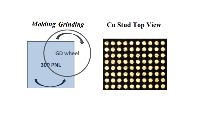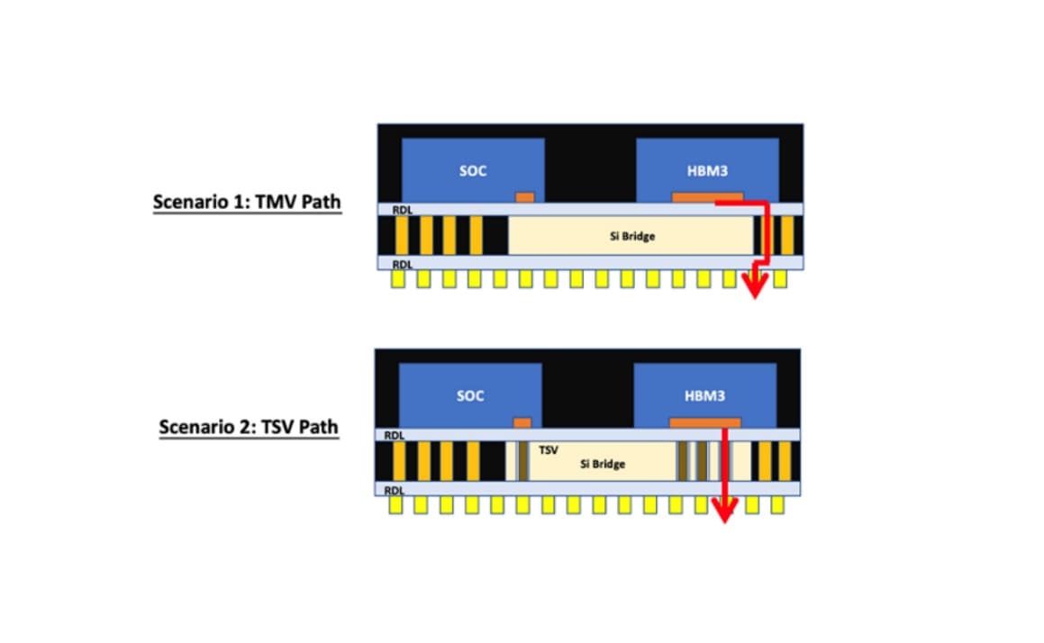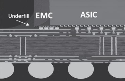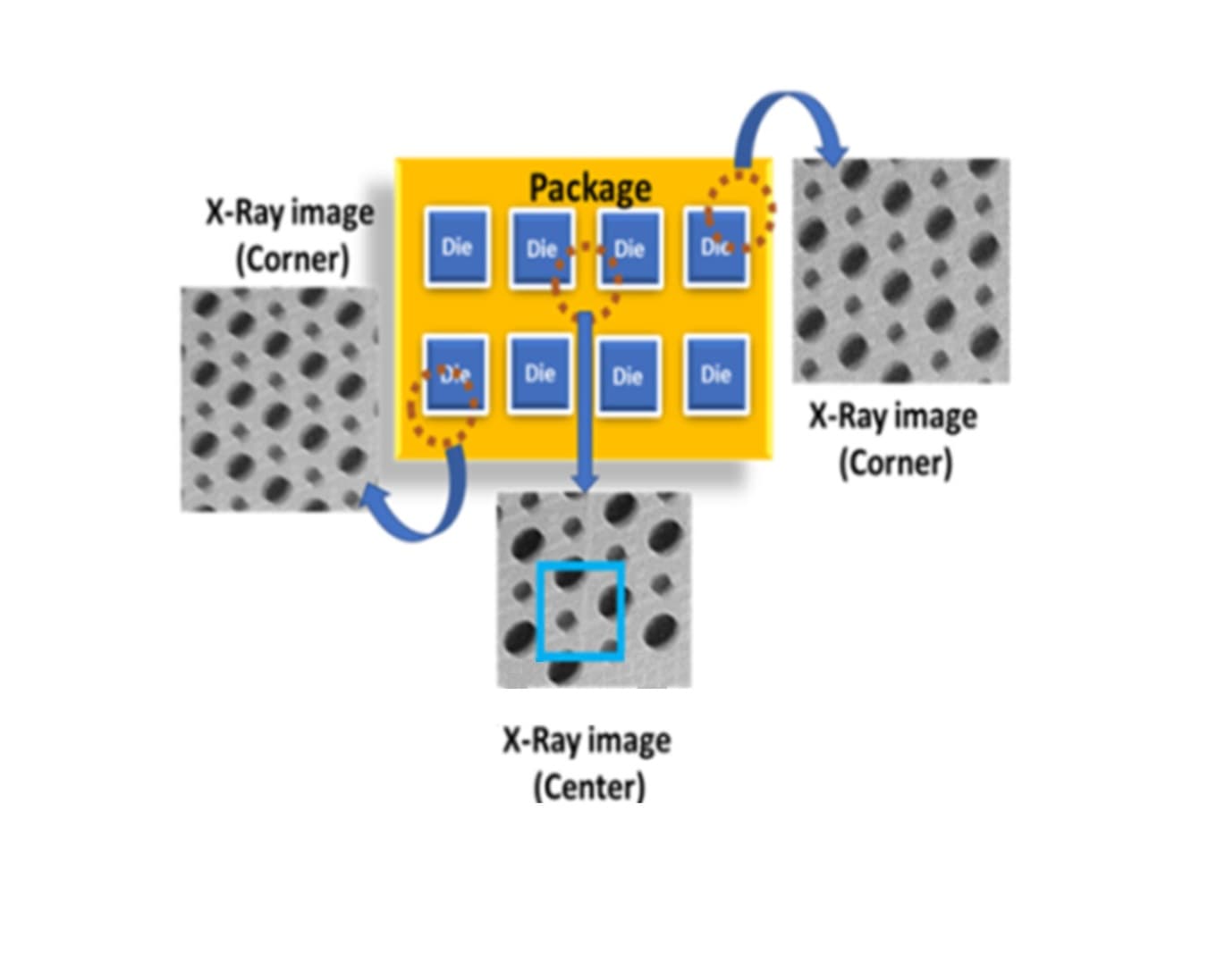
The Fifth and Sixth Generation wireless strong demands driving IC-Package development into a newly formed in higher performance, more heterogeneous integration towards commercialization, Commercialization needs an advanced fabrication platform (e.g. Panel Level Platform, PL). The promising PL IC-Package technology on outsourced semiconductor assembly/testing provides the right solution. We have successfully developed a series unprecedented PL IC-Package platform (e.g. several thousand centimeter scaling square), especially in integration of fine-pitch Re-Distribution Layer (RDL) and multi-size micro-bump. And to reduce impacted PL warpage to micro-bump connection issue, we also have built a newly curvature equation to match selections on glass carrier geometry. The AI deep learning technology proposed on PL IC-Package, our contribution is implementation of AdaGrad scheduler in Convolutional Neural Network (CNN) deep learning and implementation in advanced Automated Optical Inspection (AOI) image judgments. At the present time, we have accomplished a large area of Panel Platform for advanced IC-Packages with high complexity integration.
Published in: Microelectronics Reliability Volume 136, September 2022, 114657