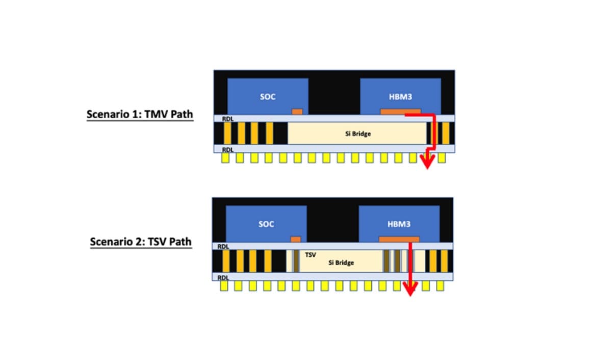
As the demand for high-performance computing (HPC) continues to rise, processor designs are evolving towards chiplet integration and ASIC-HBM architectures, leveraging high-density interconnection technologies. While wafer-level fan-out packaging (FOWLP) has become a widely adopted solution, it faces challenges such as warpage control, complex processes, and carrier utilization limitations. To address these challenges, panel-level fan-out packaging (FOPLP) has emerged as a promising alternative.
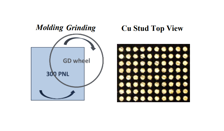
FOPLP not only offers a higher carrier utilization ratio compared to wafer-level processes but also enhances material efficiency. By reducing handling and transfer time, panel-level manufacturing can achieve higher throughput, leading to cost advantages and improved scalability. Our research presents a 300mm panel-level fan-out solution specifically designed for chiplets integration in HPC applications.
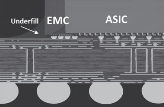
To further enhance patterning precision in panel-level processing, we have implemented an innovative Laser Direct Imaging (LDI) technique. Additionally, we investigated key factors influencing panel warpage, chip-on-panel solder joint integrity, and process optimization. The results demonstrate the successful implementation of Fan-Out Chip Last technology on a 300mm panel platform, achieving higher density, larger module sizes, and improved reliability.
These advancements make 300mm panel-level fan-out an attractive solution to meet the evolving demands of next-generation HPC and AI applications. After rigorous stress testing and structural analysis, our Test Vehicle-1 (FOPLP including 10 chiplets (SoC-1 and SoC-2) integrated with 10 Si bridge dies) exhibited excellent adhesion with no delamination across all interlayers, while Test Vehicle-2 (FOPLP including SoC-1 and SoC-2 die integrated with multiple-layer RDL) also passed reliability tests, confirming exceptional interlayer quality.
Published in: 2025 IEEE 75th Electronic Components and Technology Conference (ECTC)