2.5D
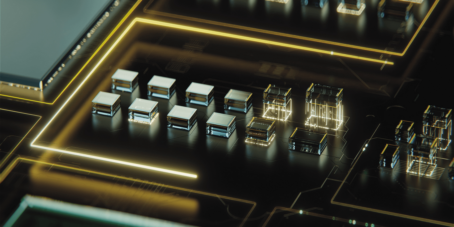
Two or more active chips sit side by side on a silicon interposer, giving extremely high die-to-die interconnect density.
Solutions
Stacking and side-by-side die integration for the bandwidth and efficiency that AI, 5G and HPC demand.
As 5G, AI and high-performance computing spread, demand keeps rising for chips with more performance, lower latency, more bandwidth and better power efficiency. 2.5D and 3D technologies deliver on all four.
ASE is an established leader in 2.5D, with pioneering solutions that helped bring advanced ASIC and HBM products to market. To keep that momentum, ASE is adding high-density Fan-Out technology for die stacking and multi-die solutions, from high-density data centers to consumer and mobile devices.

What is it
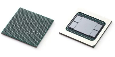
2.5D / 3D are packaging methodology for including multiple IC inside the same package. In recent years, 2.5D and 3D have become an ideal chiplet-integration platform thanks to their very high packaging density and energy efficiency. ASE is a pioneer here, and launched the world's first mass production of a 2.5D IC package with High Bandwidth Memory (HBM).
Two or more active chips sit side by side on a silicon interposer, giving extremely high die-to-die interconnect density.

Active chips are stacked, for the shortest interconnects and the smallest package footprint.

ASE's 2.5D/3D solution integrates GPU, CPU and memory alongside a decoupling capacitor.
A silicon interposer with Through-Silicon Vias (TSV) bridges the fine-pitch gap between the assembly substrate and the IC, and keeps the pad-pitch scaling path open without being limited by substrate technology.
2.5D/3D IC packaging is used mainly to integrate HBM in:
In the chiplet era, 2.5D and 3D will play a growing role in CPUs, mobile application processors, silicon photonics, display-driver ICs and more.