Solutions
FOCoS-Bridge
Overview
Tiny silicon bridges embedded in a fan-out package for interposer-class die-to-die links, at lower cost.
AI now reaches nearly every industry, from autonomous vehicles to medical diagnostics, and its convergence with HPC keeps pushing demand for data transfer. FOCoS-Bridge is built to meet that need for higher bandwidth and faster data rates. It uses highly integrated fan-out structures to get past the limits of traditional electrical interconnects, enabling high-speed, low-latency, energy-efficient communication between processors, accelerators and memory.


What is it
What is FOCoS-Bridge?
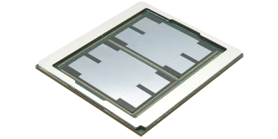
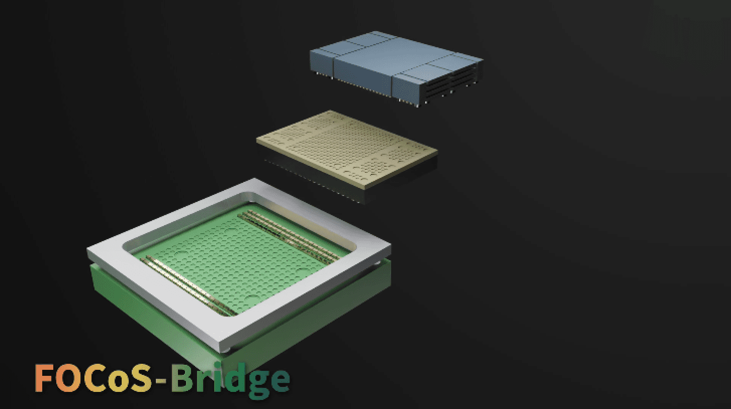
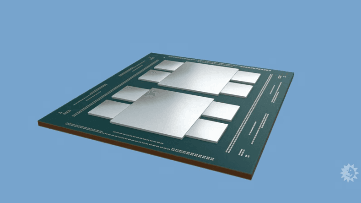
Part of the ASE VIPack™ platform, FOCoS-Bridge (Fan-Out-Chip-on-Substrate-Bridge) uses tiny silicon pieces with routing layers as in-package interconnects between chiplets, for example a GPU and High Bandwidth Memory (HBM). The silicon bridges are embedded in the fan-out RDL layer.
It is positioned as an alternative to 2.5D packages that use a full silicon interposer. Like 2.5D, it gives the ultra-fine-pitch interconnection needed to relieve memory-bandwidth bottlenecks, but it uses silicon only in the specific areas where two chiplets connect.
Supported interconnect standards
- XSR
- BOW
- OpenHBI
- AIB
- UCIe
Fabrication process
The flow builds the bridge into the fan-out package in four stages:
- A — attach the Si bridge die (with micro-bumps) to a wafer carrier, plate Cu posts, run a first molding, grind to expose the Cu posts and micro-bumps, then form the RDL layers.
- B — attach the ASIC and HBM dies, underfill, then run a second molding.
- C — remove the wafer carrier, form C4 bumps, and saw the molded wafer into individual fan-out packages.
- D — attach the fan-out package to an organic substrate using a conventional flip-chip process.

Benefits
FOCoS-Bridge matches the electrical, signal and power integrity of a silicon-interposer solution, but at lower cost and with no reticle-size limit.
It is highly scalable and delivers high-density D2D interconnection with submicron L/S, high I/O counts and high-speed signal transmission for AI and HPC.
The silicon bridge die reaches a die-edge linear density (wire/mm/layer) an order of magnitude higher than a traditional organic flip-chip package. It also lays the foundation for embedding passives and active chips in the fan-out package, with options for decoupling-capacitor integration (better power delivery) and active dies for direct access to memory, I/O and more.
Applications
FOCoS-Bridge helps advance AI, deep learning and scientific simulation.
By using computing resources more efficiently and accelerating data-heavy workloads, FOCoS-Bridge helps advance AI, deep learning and scientific simulation. Typical uses:
- Multi-die and HBM integration for AI, data center, server and networking
- Memory and passive integration for APU/CPU/GPUs and chiplets across AI, data center, mobile, automotive processors, communication infrastructure and networking
Tech Brief
Download Our Tech Brief
To download the FOCoS-Bridge Tech Brief, please complete the following form: