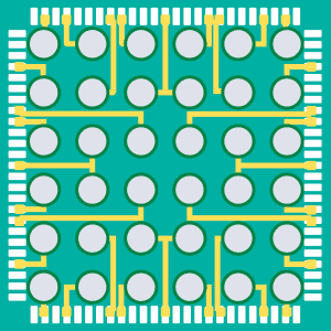
Fan-In WLP
All RDL traces are routed in towards the center of the die
Solutions
Fan-out is any package whose connections fan out past the chip surface, enabling more external I/O.
Dies are embedded in an epoxy mold (no substrate or interposer), positioned on a reconstituted wafer or panel, then given an RDL and solder balls. As a true chip-scale WLP, it avoids Fan-In WLP's die-surface I/O limit by redistributing I/O onto the over-mold.
All RDL traces are routed in towards the center of the die
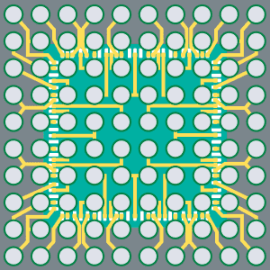
RDL traces are routed both inwards and outwards beyond the limits of the die
Fan-out shrinks the die footprint, integrates multiple dies, and enables true SiP.
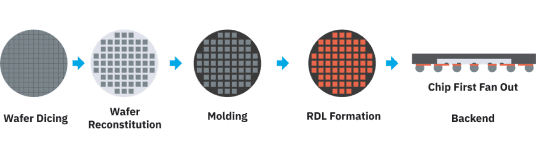
Chips embedded first, then the RDL. Lower-cost, low-I/O; but die shift, protrusion and warpage limit complex multi-chip/SiP use.
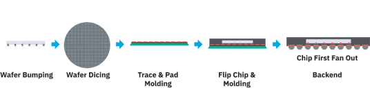
RDL pre-formed on the carrier, then chips added by flip-chip bond. Fewer KGD concerns, ultra-fine pitch (e.g. 2 µm) and better electrical performance.
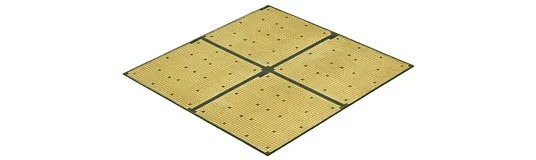
A rectangular panel carrier instead of a round wafer, for higher area utilization and lower cost, especially on large packages.
Packaging offerings
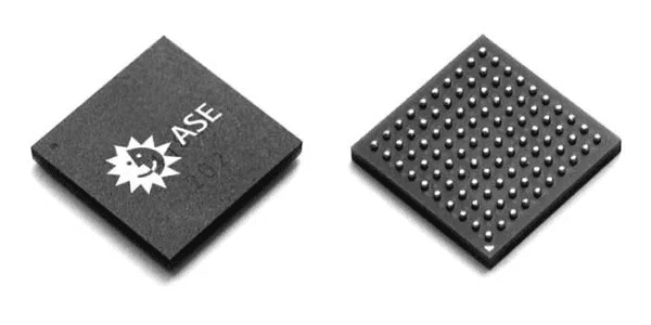
eWLB (embedded wafer-level ball-grid array), also known as ASE aWLP: Chip-First, Face-Down, licensed from Infineon.
BB, RF, Codec, Car Radar.
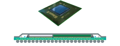
FOCoS (Fan-Out Chip on Substrate): ASE in-house developed technology.
Networking, Server.

M-Series: Chip-First, Face-Up, licensed from Deca Technologies.
RF, BB, PMIC, Codec.
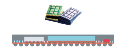
FOSiP (Fan-Out System in Package)
RF, FEM, Power, MCU.
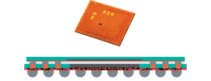
FOPoP (Fan-Out Package on Package)
AP & Memory.
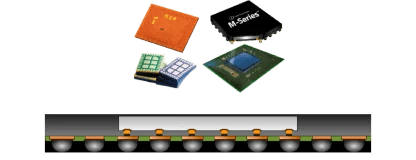
Panel-level Fan-Out uses 300 × 300 mm panels for high-density Chip-Last and 600 × 600 mm panels for low-density Chip-First solutions.
RF, FEM, Power, Server.
Mobile drives fan-out today, across PMICs, RF, baseband processors and high-end networking.
 Automotive radar (76–81 GHz)5G backhaul (>20 GHz)5G fronthaul (>20 GHz)WiGig (60 GHz)Antenna in Package (AiP)