Simulation acceleration
Cuts design-iteration time by more than 90%, taking a 14-day process down to about 30 minutes, within defined design parameters.
Solutions
An AI-driven co-design platform that cuts advanced-package design cycles from weeks to hours.
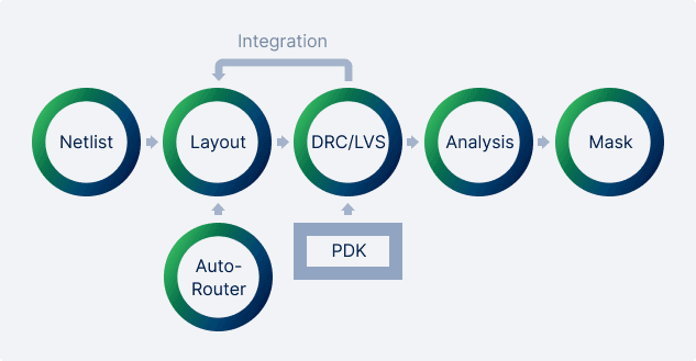
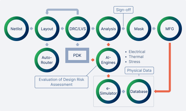
Building on the original Integrated Design Ecosystem™, IDE 2.0 is a major upgrade in advanced-package co-design. It brings artificial intelligence into the flow to speed up design iterations, sharpen chip-package interaction (CPI) analysis, and get complex AI and HPC products to market faster.

The IDE 2.0 workflow can cut overall design-and-analysis cycle time from weeks to hours. Three highlights stand out:
Cuts design-iteration time by more than 90%, taking a 14-day process down to about 30 minutes, within defined design parameters.

Improves accuracy across electrical, thermal, warpage/stress and reliability domains at once.

Generates predictive risk assessments in about 60 seconds, enabling real-time design optimization.
| Request | Simulation | Reporting | Review | |
|---|---|---|---|---|
| Electrical | 0.5 days | 1–2 days | 5 mins | 5 mins |
| Thermal | 1–3 days | 2–7 days | 1–2 days | 1–2 days |
| Stress | 1–3 days | 2–7 days | 1–2 days | 1–2 days |
| Request | Simulation | Reporting | Review | |
|---|---|---|---|---|
| Electrical | <1 min | 15 mins | 5 mins | 5 mins |
| Thermal | 10 mins | 1–20 mins | 1 min | N/A |
| Stress | 10 mins | 20 mins | 1 min | N/A |
Through a new cloud-based e-Simulator, IDE 2.0 uses AI engines to run CPI predictive risk assessments and to optimize design, analysis and manufacturing data.
It adds an AI-driven feedback loop that continuously connects design and analysis in real time, so teams can innovate faster while managing growing complexity across multi-die, chiplet and heterogeneous-integration designs. Combining multiphysics simulation, real-world data and AI insight improves speed, precision and reliability, helping customers make smarter, data-driven design decisions.
Tech Brief
To download the Integrated Design Ecosystem™ Tech Brief, please complete the following form: