Shorter interconnection
- Better signal integrity, less attenuation
- Addresses range and propagation challenges at higher frequencies
Solutions
Overview
Antenna in Package (AiP), or antenna on Package (AoP), has become the mainstream antenna-packaging technology for millimeter-wave (mmWave) applications. Through its leadership in SiP, ASE offers a full suite of AiP capabilities, from system design, software development and module testing to electro-thermal simulation, so customers can build smaller, higher-performance, lower-power and more cost-effective mmWave products.
5G delivers better latency, reliability, efficiency and capacity than earlier wireless. In 4G and sub-6 GHz devices, antennas are discrete (printed on the PCB or assembled near the RF front-end). Because antennas are much smaller at mmWave frequencies, the antenna can be integrated directly into the package, placing the transceiver closer to the antenna to boost the signal.
What is It
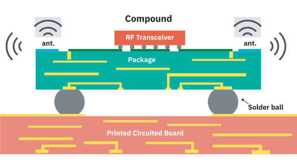
It can be further integrated with front-end components, power amplifiers or low-noise amplifiers, switches, filters, even a PMIC, into an antenna module using SiP techniques such as double-side molding, selective molding, passive integration and EMI shielding. A typical FCBGA AiP has the RF chip on a package substrate with solder balls to the main PCB, an antenna array on top, and flip-chip connections to reduce interconnect loss.
Advantages
ASE mmWave AiP offerings

RF chip on the bottom of a BGA substrate, antenna array on top. ASE designed a 28 GHz AiP with a 2×2 stacked-patch array on a low-loss multilayer organic substrate.
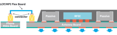
For smartphones: RF chip on a multi-layer (typically >12-layer) antenna board with the array on the bottom, plus a connector that carries multiple high-frequency signals to the main board via a flex PCB.
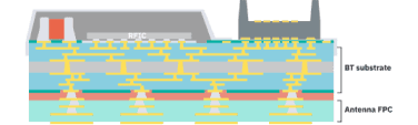
RF chip on a hybrid substrate: a BT substrate plus an antenna flex PCB built from low Dk/Df materials for the lowest signal loss at high frequency.
Applications
Because the antenna can be small enough to fit into a small package, AiP is widely used in high-frequency applications: 60 GHz radios and gesture radars, 77 GHz automotive radars, 94 GHz phased arrays, 122 GHz imaging sensors, 300 GHz wireless links, and 5G mmWave networks (28, 39, 60, 77 and beyond 90 GHz).
Measurement
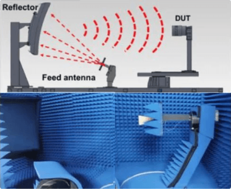
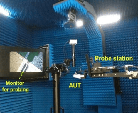
Over-the-air (OTA) testing of 5G beamforming antennas is a challenge. With Keysight Technologies, ASE developed an AiP measurement system with best-in-class measurement integrity and high repeatability, using a Compact Antenna Test Range (CATR) chamber.