ASE semiconductor packaging substrate

Other Services

Packaging Substrate

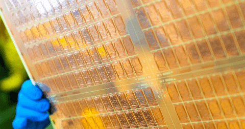
ASE designs and manufactures advanced packaging substrates that connect semiconductor dies to the package and system board, integrating substrate and assembly expertise for reliable quality, fast cycle time, and high-volume ramp.

A value-critical part of the package

As package dimensions shrink and performance rises, substrates carry more complex signal, power, and ground structures while accounting for a larger share of package value and performance.

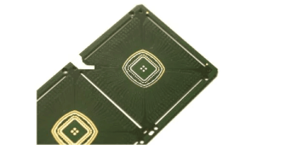
ASE integrates assembly and substrate technologies to deliver a broad range of wire-bond BGA and flip-chip products. Stub-less etch-back, advanced selected-gold, and double-pattern-sputter options support high-frequency and high-performance designs.

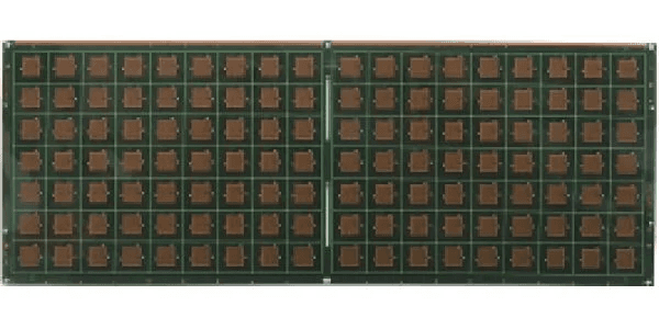
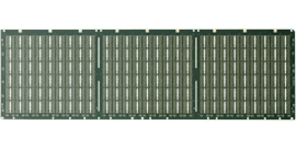
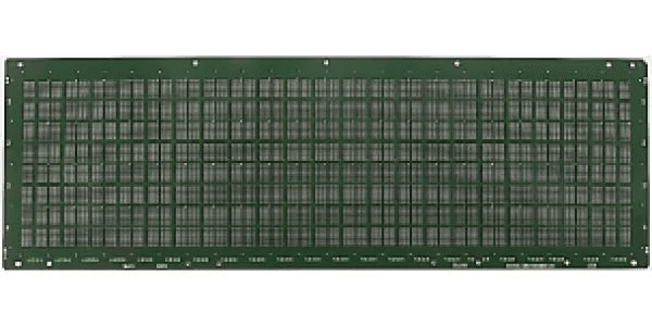
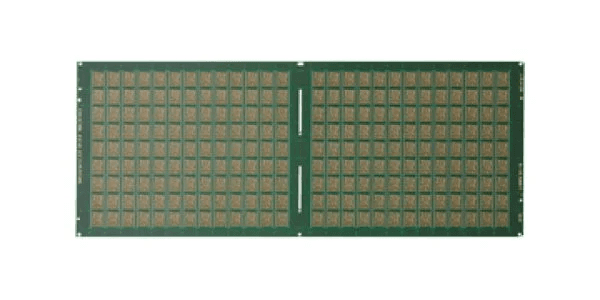
ASE plastic BGA substrate
img packaging substrate 1
img packaging substrate 2
img packaging substrate 3
Features diagram

ASE Packaging Substrate offerings

Plastic BGA substrate

Multilayer glass-fiber laminate substrates for high-speed, high-power, automotive, communications, graphics, and medical packages.

Flip-chip CSP substrate

Coreless and embedded-layer structures with fine-line capability for application processors, modems, connectivity, Bluetooth, and networking.

BOC and LPDDR

Short-wire, cost-effective memory substrates for high-frequency and low-power DRAM products.

Module substrate

Coreless multilayer substrates that integrate active and passive devices for wireless, wearable, fingerprint, GPS, RF, TWS, and IoT modules.

a-S³ single-sided substrate

A single-sided build-up flow targeting lower profile and lower cost for application processors, networking, and connectivity.

Embedded Trace Substrate (ETS) diagram

Integrated design and manufacturing

In-house design, stable high-volume capacity, and close integration with packaging operations allow ASE to shorten cycle time, support customer ramps, and align substrate rules with the electrical, thermal, reliability, and cost goals of the final package.

  • Thin-core and coreless options
  • High-density interconnect
  • Automotive-grade quality
  • Advanced surface finishes
  • Flexible multilayer signal, power, and ground design
Features diagram
Features diagram
Features diagram