Solutions
3D System-in-Package (3D SiP)
Overview
A three- or four-side assembly structure that shrinks package size further while adding more function.
Driven by IoT, edge computing, wearables and next-generation wireless, more electronic components are assembled into a single unit to provide the functions of a system or subsystem. Double side molding (DSM) first addressed this by assembling die on both sides of a substrate. To shrink the package further and add more function, ASE developed 3D System-in-Package, with a three- or four-side assembly structure.
What is it
What is 3D SiP?
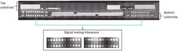
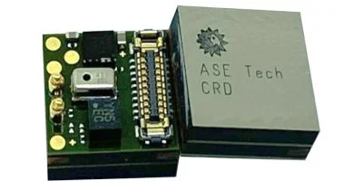
3D SiP is a very-high-density assembly structure with three- or four-side assembly on top and bottom substrates, interconnected by signal-routing interposers in between to raise packaging density. Active components (fcCSP, WLCSP, silicon die, MEMS) and passive components (resistor, capacitor, inductor, crystal or oscillator) can mount on both sides of both substrates.
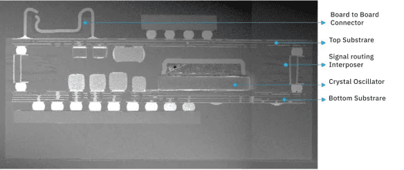
Compared with double-side SiP, 3D SiP reduces area by more than 13% while adding less than 10% thickness.
Assembly process
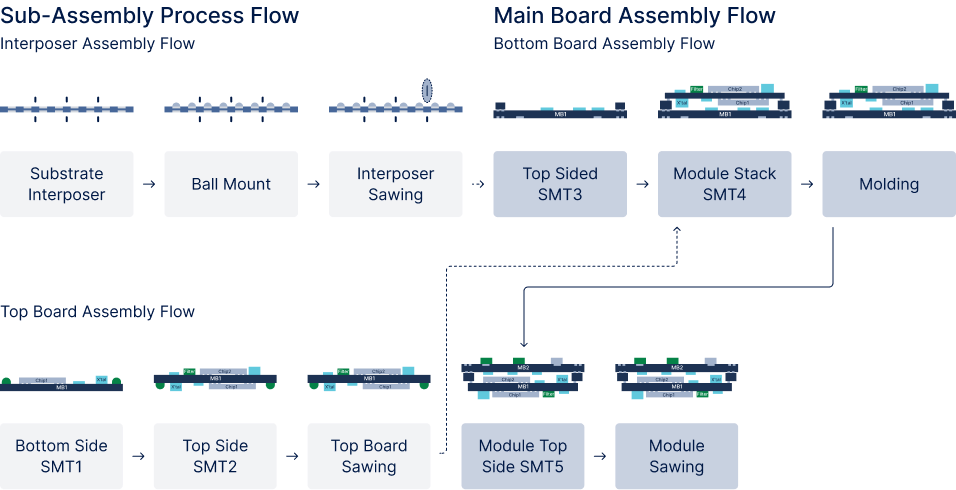
The 3D SiP assembly process has three phases:
interposer assembly, top-board assembly, and bottom-board (module) assembly. Methods include SMT, molding, sawing and shielding.
Key advantages
- Smaller form factor
- Allow highly integrated electronic functionalities
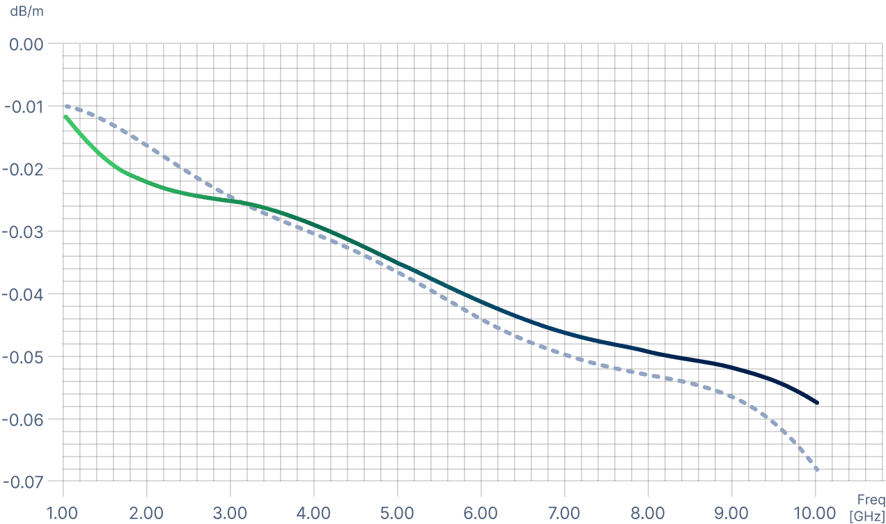
- Better electrical performance
Insertion Loss
Applications
Miniaturization and more function integration
3D SiP suits package sizes from 6×6 mm² to 30×30 mm², for wearables (watch, earphone), wireless chargers, RF front-end modules and sensor systems. Its main advantages, miniaturization and more function integration, make it a good platform for consolidating heterogeneous chips into a small form factor.