Solutions

Wire Bond BGA

Overview

A BGA places output pins as a solder-ball matrix, using the whole substrate to route interconnects.

Traces run on laminated (BT) or polyimide-film substrates; lower ground/power inductance and optional heat sinks or thermal balls suit high-power, high-speed ICs.

Versus traditional SMT packages

Higher interconnect density

Lower assembly cost

Self-alignment during reflow

Lower profile

Easier thermal & electrical management

Easier routing

Packaging offerings

Wire Bond BGA offerings

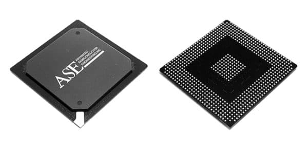
ASE PBGA wire bond package

BGA packages that use plastic (epoxy molding compound) as the encapsulation. Per JEDEC, PBGA has an overall thickness of over 1.7 mm.

Applications

  • Graphics, PC chipsets, microprocessors/controllers, PLDs
  • Communications, networking, DSPs
  • ASIC and gate arrays, memory packages

Features

  • 15×15–45×45 mm; 119–1520 balls; JEDEC MS-034 outlines
  • High interconnect density, low profile, self-alignment during reflow
  • Easy thermal/electrical management and routing; low assembly cost; good power dissipation; lead-free available; full in-house design


More Solutions

We use cookies to run this site and, with your consent, to measure how it is used. See our Cookie Policy and Privacy Policy.