
Silicon Photonics
Overview
AI is generating unprecedented amounts of data and intensifying the need for energy efficiency. Data-center hardware is being reinvented to accelerate compute and cut power while keeping latency low. Silicon photonics has emerged to help, shifting data transmission from copper to light. Co-packaged optics (CPO) is a packaging approach that integrates the optical components tightly, and ASE has demonstrated CPO that improves energy efficiency and scalability for AI.
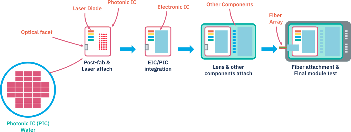
SiPh and its advantages
Silicon photonics (SiPh) is a medium for transmitting light. It works within the existing CMOS ecosystem, front-end and back-end, so it can build high-density photonic integrated circuits (PICs) that deliver optical functions like filtering and modulation on a compact, cost-effective chip. Compared with electrical ICs, which hit signal-integrity limits at high speed, SiPh offers higher bandwidth and greater energy efficiency.
Silicon photonics integrates photonic functions with the CMOS manufacturing ecosystem. Dense photonic integrated circuits can filter, modulate, and route light in a compact and cost-effective chip.
Where conventional electrical links face growing signal-integrity and power challenges at high speed, optical transmission provides a path to higher bandwidth and stronger energy efficiency.
How fiber-optic integration is evolving
SiPh-based pluggable optical transceivers up to 800 Gbps are already commercial. Instead of a front-panel transceiver, the optical engine can sit around the ASIC package as on-board optics (OBO), supporting up to 1.6 Tbps. Beyond OBO, co-packaged optics and optical I/O shorten the electrical path further with tighter assembly integration, delivering even higher bandwidth with better energy efficiency (pJ/bit) and lower cost ($/Gbps) than pluggable optics.
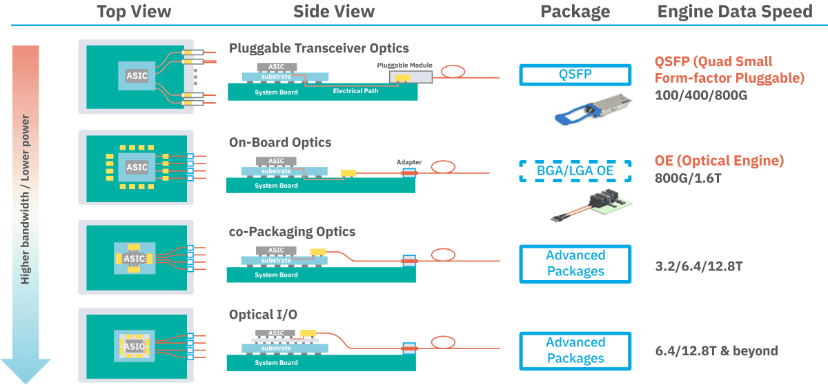
Technical building blocks
SiPh needs extra care in the process flow to protect optical performance. Key technologies that enable pluggable, on-board and co-packaged optics:
Optical performance requires package and assembly processes developed specifically for photonic products.
- Post-fab wafer-level bumping and Si-etch process
- High-accuracy laser die bonding
- Advanced 2.5D/3D packaging (TSV / FO / CoW) for EIC and PIC die integration
- Wafer-level optical probing to find known-good SiPh PIC dies
- Optical-component assembly evaluation for future OBO and CPO
- MCM module assembly
- Pluggable, on-board, and co-packaged optics for hyperscale data centers, HPC, AI, and machine learning
Applications
Silicon photonics enables heterogeneous on-board optics, co-packaged optics and optical-I/O packaging, for:
- Hyperscale Data Center
- High-Performance Computing (HPC)
- Artificial intelligence & Machine learning (AI & ML)
More Solutions
 Next-Generation Advanced PackagingPanel-Level Packaging
 Advanced PackagingHeterogeneous Integration
 Vertically Integrated PackagingVIPack™
 Integrated Design Ecosystem™Integrated Design Ecosystem
 Advanced RDL Packaging2.5D and 3D IC Packaging
 Advanced RDL PackagingFOCoS
 Advanced RDL PackagingFOCoS-Bridge
 Advanced RDL PackagingFOPoP
 System-in-PackageSystem-in-Package
 System-in-PackageDouble Side Molding
 System-in-PackageFan-Out SiPSystem-in-Package3D SiPSystem-in-PackagepowerSiP™
 System-in-PackageAntenna in Package
 System-in-PackageEmbedded Die Substrate
 System-in-PackageMEMS and Sensor Packaging
 Other PackagingLeadframe Packaging
 Other PackagingWire Bond BGA
 Other PackagingFlip Chip Packaging
 Other PackagingWafer Level Packaging
 Other PackagingBumping ServicesOther PackagingFan-Out Packaging
 Other ServicesTest Services
 Other ServicesPackaging Substrate
 Other ServicesPackage Design
 Other ServicesSubstrate Design
 Other ServicesLab Services