Solutions
Wafer Level Packaging
Overview
ASE offers a broad range of wafer-level packages, from chip-scale to SiP and heterogeneous integration.
They deliver the thinnest profiles, lower power and high performance, for everything from client devices to cloud infrastructure and emerging VR/AR, autonomous driving and robotics.
Packaging offerings
ASE wafer level packaging offerings
Wafer Level CSP (aCSP / WLCSP)
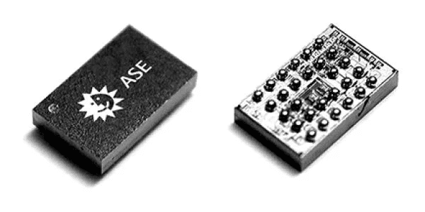
To service the fast-growing market within PDA and cell phone, this smaller chip size is essential. In 2001, ASE licensed Ultra CSP® from Kulicke & Soffa's Flip Chip Division. ASE also provided several enhanced structures called “aCSP™” by polyimide, PBO, or thicker Cu RDL to meet various customer demands. aCSP™ is a wafer level CSP package that can be Direct Chip Attached to the PCB board without any interposer. Also, aCSP™ provides the shortest electrical path from Al pad to PCB board to enhance the electrical performance. It has been broadly used in portable devices in passives, analog and logic applications, and is extending to RF applications.
Applications
- Bluetooth/Wi-Fi, RF devices, power amplifier, FM radio
- Analog devices, power & voltage regulators, microcontrollers/integrated passives
- Cell phones and system boards, GPS, EEPROM
Features
- Real chip size (smallest, thinnest and lightest)
- High-density interconnection
- High-speed data processing
- Batch process-assembly processed in wafer form
- Wire-bond type die can be directly switched to aCSP
Product Offerings
- aCSP: Through ball drop process
- WLCSP: Through ball printing/plating process
Advanced Technology under Development
- Wafer technology: Qualification for 22 and 16nm wafer
- Ball pitch: 300um
- Ball size: 150um ball drop
- Grinding: Die thickness 150um
- Plated RDL line/width: 10/10um; 8/8um
- Plated RDL thickness: >=7um
- Sawing: Laser sawing
Advanced Wafer Level Package (aWLP)
A die-down fan-out package with mold compound surrounding the die, adding I/O capacity without a substrate while improving electrical and thermal performance.
Wafer Level Integrated Passive Device (WL IPD)
A low-loss glass process for custom RF passives such as resonators, filters, diplexers, baluns, transformers, and inductors.