A new era for chip scaling
The old path of shrinking devices and cutting cost at every node is running out of room. Packing more transistors onto a single monolithic IC gets harder and more expensive at each generation.
Solutions
Overview
The old path of shrinking devices and cutting cost at every node is running out of room. Packing more transistors onto a single monolithic IC gets harder and more expensive at each generation.
Putting every function on one chip (a system-on-chip, or SoC) is possible, but it drives up cost and design complexity as the chip grows.
Heterogeneous integration uses advanced packaging to bring together devices that were each designed and manufactured with the process best suited to them, assembled in the most optimized way.
What is it
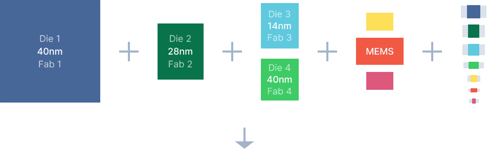
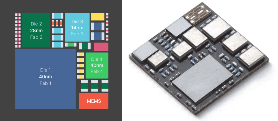
Heterogeneous integration is the assembly of separately manufactured components into a higher-level package (a System-in-Package (SiP)) that together delivers more functionality and better operating characteristics than the parts alone.
The core idea is to place multiple dies in the same package, so the package performs an advanced function in a small form factor.
Why it matters
Conventionally the industry squeezed everything onto one monolithic chip, but that chip keeps getting bigger and more expensive. Heterogeneous integration solves this by combining chips of different process nodes and technologies, which keeps functional density rising and cost per function falling.
 Higher performance
Lower latency
Smaller size
Lighter weight
Lower power per function
Lower cost
Technology building blocks
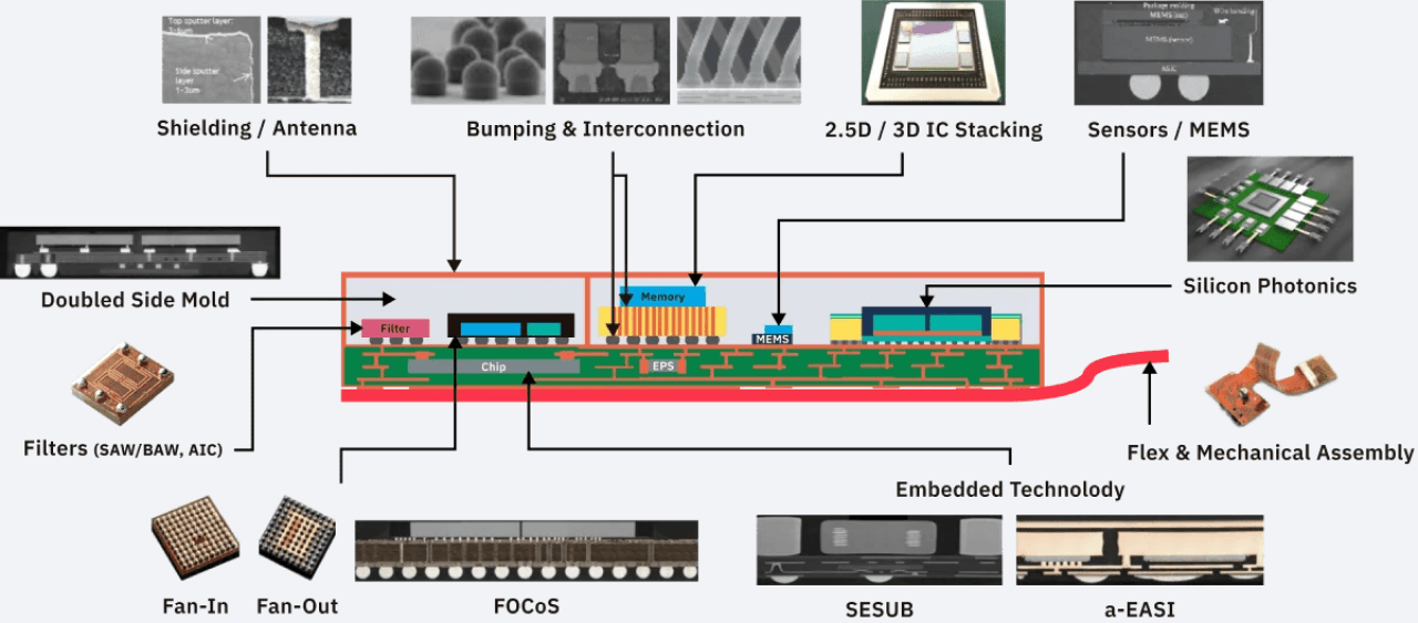
HIR
Emerging technologies such as AI, 6G, edge, cloud and data center, autonomous vehicles and wearables hold real promise for people worldwide. The HIR maps the future of system-level integration and the advanced packaging needed to get there.
ASE's Dr. William (Bill) Chen leads the HIR initiative, alongside Dr. Bill Bottoms (3MTS, IEEE EPS), Tom Salmon (SEMI), S. Iyer (IEEE EDS), A. Helmy (IEEE Photonics) and Ravi Mahajan (ASME EPPD). ASE contributors include Rich Rice, CP Hung, John Hunt and Mark Gerber, with many more from across the electronics community.
Solution platform
Ultra-compact, high-capacity, low-power modules with controller and sensor integration, built for the miniaturization needs of AI, IoT and mobile devices. ASE has also developed business models that actively grow the SiP ecosystem.
ASE's SiP and MEMS solutions draw on established IC assembly capabilities: copper wiring, flip-chip packaging, wafer-level packaging, fan-out wafer-level packaging, 2.5D/3D IC and embedded-chip packaging.
 Mobile devices
 IoT
IoT High-performance computing
 Internet of Vehicles (IoV)