Solutions
Bumping
Overview
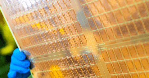
Wafer bumping forms solder or Cu-pillar bumps on whole wafers before dicing, connecting die to substrate.
These bumps (eutectic, lead-free, high-lead or Cu pillar) carry the electrical, mechanical and thermal load of a flip-chip package. Flip chip cuts signal delay and package size versus wire bonding, which has spread it from niche high-end to mainstream consumer and mobile.
Capabilities
State-of-the-art 200 mm and 300 mm bumping in Kaohsiung, running since 1999.
From 2017 to 2021, ASE processed over 5 million 8-inch wafers (60+ customers) and over 5.3 million 12-inch wafers (110+ customers) in its plating and Cu-pillar facilities, growing about 10% a year, plus over 1.1 million fan-out molding wafers since 2017. It bundles substrate design and manufacturing, wafer sort, bumping, backside grind and marking, flip-chip assembly and final test into a turnkey solution.
Advanced technologies
Working with leading IDMs and top foundries on next-generation bumping.
 Polyimide repassivationRDL5 nm / 4 nm Cu low-K wafer bumping
Cu pillar
Cu-pillar bumps are the most effective route to fine-pitch flip-chip interconnection.
As devices trend toward smaller, thinner, lighter and higher-performance designs, bump size shrinks and fine pitch becomes essential. ASE's Cu-pillar bumps in flip-chip packaging are the most effective method for fine-pitch interconnection across these package types.
Applications
Consumer: camcorders, digital camera, DVD, WiMAXComputer: voltage regulators, high-speed memory, card, PC peripheralsTelecom: pagers, cellular handsets, GPSFeatures
Fine pitch possible below 45 µmMore stable chip-to-substrate standoff; higher elastic modulusGood electrical performance and high reliability — Cu-pillar bumps resist electromigration and thermal fatigueNo bump bridging between adjacent bumps; uniform current distribution; lower cost