FOCoS-CF (Chip First)
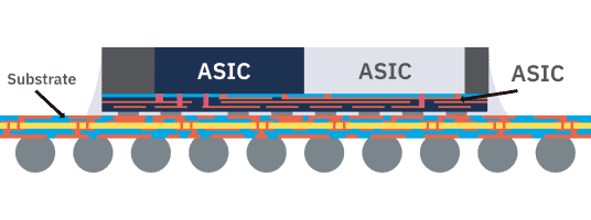
Two ASIC chiplets face down, connecting directly to the RDL through Cu vias, with no micro-bumps between the Si dies and the fan-out RDL (L/S 2/2 µm).
Solutions
A fan-out package on a BGA substrate that links multiple chiplets at high density, without a silicon interposer.
Chiplet integration for high-performance computing (HPC) is a top priority, and it needs reliable advanced packaging that makes the critical die-to-die connections as efficiently as possible. ASE's high-density FOCoS solutions do exactly that.

What is it
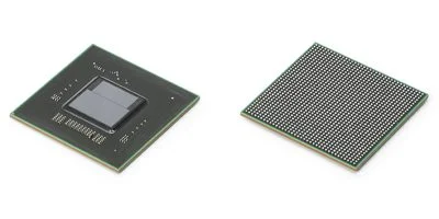
The fan-out package carries a redistribution layer (RDL) that creates short die-to-die (D2D) interconnections between multiple chips. That fan-out package is treated as if it were a single die, then flip-chip mounted onto the BGA substrate.
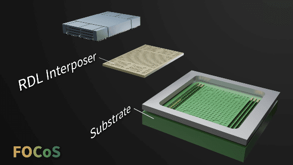
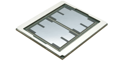
Two ASIC chiplets face down, connecting directly to the RDL through Cu vias, with no micro-bumps between the Si dies and the fan-out RDL (L/S 2/2 µm).
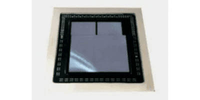
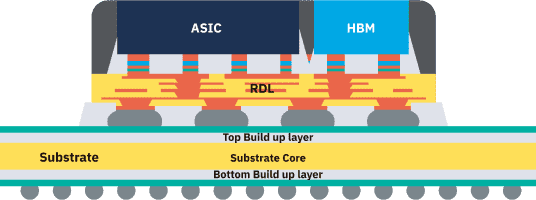
Three chiplets (1 ASIC + 2 HBM) side by side, connected through the RDL (L/S 2/2 µm) and Cu micro-bumps.
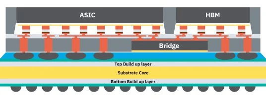
Two chiplets (1 ASIC + 1 HBM); a Si bridge die (L/S 0.6/0.6 µm) is embedded in the fan-out RDL (L/S 10/10 µm) to link them.
FOCoS removes the need for an interposer, which lowers package cost. It also has less insertion loss, better impedance control and lower warpage, for better electrical performance.

ASE's FOCoS options give a wide choice.
FOCoS suits large package sizes and high I/O density (>1000 I/Os) for networking and server products. The chip-last version can package ASICs and HBM. Together, ASE's FOCoS options give a wide choice for chiplet integration in HPC and AI/ML.

A fully validated Assembly Design Kit.
With Siemens Digital Industries Software (OSAT Alliance Program), ASE developed a fully validated ADK that lets customers create and evaluate complex FOCoS packages in an easy-to-use, data-robust graphical environment, before and during physical design.
Built on Siemens Xpedition Substrate Integrator and Calibre 3DSTACK and integrated with ASE's design flow, the ADK cuts FOCoS planning and verification time by roughly 30 to 50 percent per design iteration, so ASE and customers can co-design packages and close verification issues quickly.