Solutions
FOPoP
Overview
A fan-out, RDL-based package-on-package that is thinner and faster than interposer-based PoP, for mobile and networking.
Today's portable products, from smartphones to tablets and wearables, need packaging that adds functionality and performance in a smaller footprint at lower cost. Conventional interposer-based Package-on-Package (PoP), which via-stacks two or more packages, integrates multiple functions with flexibility, better cost and faster time to market.
To go thinner still and improve electrical and thermal performance, an RDL-based PoP called Fan-Out Package on Package (FOPoP) was introduced. ASE's FOPoP lowers latency and delivers strong bandwidth for the mobile and networking markets.
What is it
What is FOPoP?
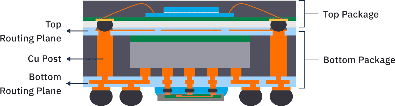
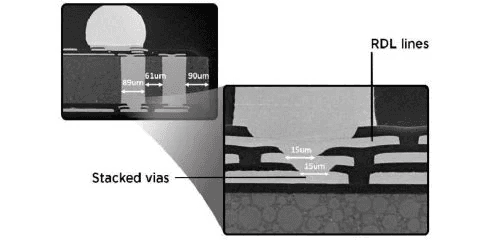
A core packaging pillar of the VIPack™ platform, FOPoP is an RDL-based package that combines a fan-out bottom package with a standard package mounted on top, using fine-pitch plated Cu posts for the through-mold vertical connections. The bottom package has two RDLs (top and bottom routing planes) joined by the Cu posts, formed with wafer-level fan-out technology for thinner, finer traces.
Fabrication in brief
The flow is similar to conventional PoP, except the bottom package is built with an RDL-first fan-out process: Cu posts are plated onto a temporary carrier before die attach, and the second routing plane connects to the Cu posts exposed from the molding by grinding.
1
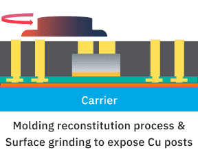
Molding reconstitution process & Surface grinding to expose Cu posts
2
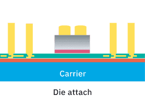
Die attach
3
Molding reconstitution process & Surface grinding to expose Cu posts
4
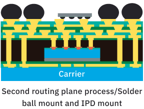
Second routing plane process / Solder ball mount and IPD mount
Benefits
Thinner, better electrical and thermal performance.
Compared with interposer-based PoP, FOPoP is thinner with better electrical and thermal performance, because the bottom package removes the interposer. Because it is still PoP, the known-good-die (KGD) issue is eased, since the top package can be burned-in and tested before mounting. Top and bottom packages can be decoupled for qualification, yield, sourcing, procurement and logistics, which cuts development time and cost.
For mobile
- Ultra-low profile, nearly 40% shorter than substrate-based PoP
- Better electrical efficiency and power for advanced silicon nodes
- Good warpage at high temperature for strong SMT yields
- Stable dielectric constant (Dk) across a wide high-frequency range
- A roadmap toward heterogeneous and homogeneous chiplet integration
For networking
- 3x shorter electrical path and up to 8x denser bandwidth (up to 6.4 Tbps per unit)
- Energy efficiency improved from 25 pJ/bit to 5 pJ/bit
- Controls losses above the 10 GHz range
- Advanced integration of PIC, controller chips and pre-alignment structures for laser, optics and fiber
- Sub-µm accuracy and better optical coupling via passive alignment
Applications
FOPoP has become a promising 3D-integration solution for several chip combinations:
- AP + Memory (4G/5G)
- ASIC + Antenna
- (5G)EIC + PIC (Networking)
It addresses application processors, mobile, automotive, antenna-in-package and co-packaged silicon photonics, and delivers strong advantages for AR, VR, MR and networking, where small size means more battery space, a better form factor and more efficient routing.
Tech Brief
Download Our Tech Brief
To download the FOPoP Tech Brief, please complete the following form: