Miniaturization & flexibility
- Frees space for other components or shrinks the whole solution
- Design moves from 2D to 3D
Solutions
Burying the die inside the substrate for a smaller, cooler, better-performing package — offered as a-EASI and SESUB.
As the market needs to pack more chips and functions, higher performance, lower power and better heat dissipation into a smaller form factor, demand for embedded die substrates (such as a-EASI and SESUB) is expected to grow worldwide. ASE offers a full turnkey embedded-die-substrate solution, drawing on its advanced packaging and test expertise and its substrate design and manufacturing capability.
What is it
Conventionally, active dies sit on top of a substrate for support and interconnect. In an embedded die substrate, the die is embedded within standard PCB material (organic laminated layers) and/or a lead frame during substrate formation, then connected to other components (MEMS or passives) through copper-plated vias and conductive traces.

a-EASI
ASE's Embedded (Chip) Technology is considered an alternative solution to achieve higher-level integration with multi-functionalities and form factor shrinkage advantages. ASE a-EASI is suitable for power electronics applications to reduce power loss and high thermal dissipation which also had robust mechanism. Embedded Technology provides SMT integration and flexible routing solution to reduce PCB size. The short connection path though Cu via structure. a-EASI applied metal lead frame to die placement which has high thermal dissipation and EMI benefit.
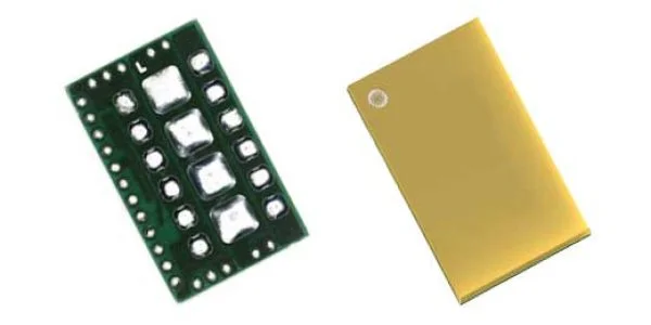
 MOSFETIGBTRegulatorPower modulesDCDCPinout: BGA/LGA/QFNIOs: Up to 100Package size: <50 (mm²)Power: 1000+ (W)Thermal: Excellent


SESUB
SESUB (Semiconductor Embedded in SUBstrate) is a technology that embeds the IC in the laminated substrate. This substrate with the thinned IC embedded can be mounted with various electronic components to form a highly integrated, multiple-function module/package. SESUB enables the micro-modularization of functional circuitry such as high-performance PMUs for smartphones as well as Bluetooth modules. SESUB has already been a proven technology by many customers and IC vendors.
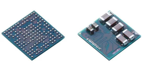 MCUFEMPMICOpticalConnectivityAudioPowerSensorProcessorImage moduleAutomotive ADASHigh-Frequency ApplicationMemoryPinout: BGA/LGAIOs: Up to 1000Package size: 200+ (mm²)Power: <20+ (W)Thermal: Good
The figure below illustrates the cross-section view of a multi die embedded module utilizing SESUB technology. The SESUB is a 1-2-1 4-layer structure which provides properties for size reduction, thermal dissipation, mechanical robustness, performance improvement. SESUB not only serves as module, but also as package with thin thickness.
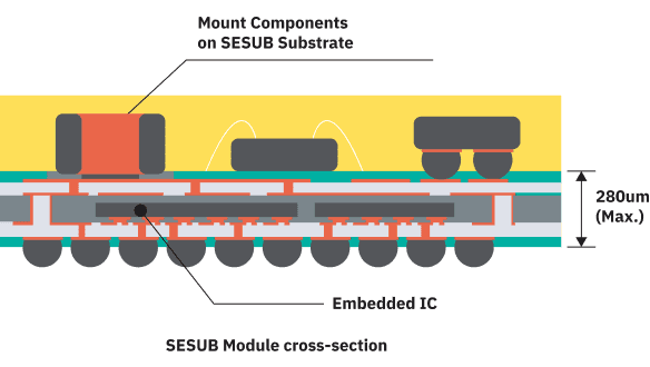 Multi-die embedded in substrateThin substrate thickness max. 280umSmall form factorLow profileEnhance heat dissipationMitigate unwanted noise radiationJEDEC MSL3 certifiedVery thin die thickness min. 50umHigh integration packageSpace savingLow noise emissionRobust copper connectionSMT on surface of substrate