Electrical verification
Assesses whether a device complies with its various operating specifications.
Solutions
Overview
Plus a broad range of test-related services: electric interface board and mechanical test-tool design, program conversion, program-efficiency improvement, burn-in testing, dry-pack, and tape & reel.
Coverage
With deep expertise in test platforms, program conversion and test-program development, ASE covers SoC, MCM and SiP testing as more functions pack onto a single chip or package.
Capabilities
Support
With deep expertise in test platforms, program conversion and test-program development, ASE covers SoC, MCM and SiP testing as more functions pack onto a single chip or package.
Assesses whether a device complies with its various operating specifications.
Assesses long-term reliability and suitability for the intended application.
Investigates when a device doesn't meet specification during verification or reliability testing.

Automation
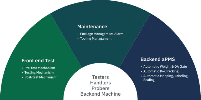
A process to rework singulated die in tape-and-reel when customers need to re-probe. It reprocesses WLCSP die packed in tape & reel: de-tape, reconfigure singulated die in a film frame, probe the singulated die, then pick-and-place back to tape & reel. The probe card is the same as production, so no new probe card is needed.
Capability
Visual inspection and electrical test of processed wafers to customer spec. Pins from ten-thousands to multi-site hundreds; wafer size 6–12 inches; probe cards (micro-spring, vertical, cantilever, membrane); temperature −40 to 125°C; digital, analog, RF and automotive devices; WLP singulated re-screen.
Logic, mixed-signal and RF devices with leads from single digits to several hundreds and frequencies up to several GHz. ASE has the largest installed test-equipment base among independent providers. Also burn-in, system-level test, visual inspection, singulated top marking, dry pack, tape & reel.
Burn-in stress for different power requirements (5–600 W) for product-lifecycle validation, especially automotive devices.