Inertial
- Gyroscope
- Accelerometer
- Magnetometer/Hall-Effect Sensor
- Combo & IMU
Solutions
Packaging that is part of the device's function, letting sensors see, hear and feel the world.
MEMS (Micro-Electro-Mechanical Systems) and sensors let us experience and interact with our surroundings. A MEMS device combines mechanical elements, sensing features and electronic circuits on a silicon substrate, gathering information by measuring mechanical, thermal, biological, chemical, acoustic, optical and magnetic stimuli. Wafer-level packaging and TSV are key enabling technologies that optimize size, functionality and performance for cost-effective integration. ASE brings extensive modeling-lab capability, including optical simulation and measurement, material measurement and stress simulation.
The rise of robotics, autonomous vehicles, smart homes, IoT, AR/VR/MR and environmental hubs is accelerating MEMS and sensor development.
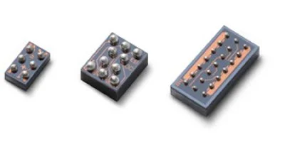

MEMS is a process technology for making tiny devices that combine mechanical and electrical components and can sense, control and actuate.
Unlike traditional packaging that only protects the chip, MEMS packaging is part of the device's function: microphones and pressure sensors need sound or pressure inlets; optical devices need materials that pass the right wavelengths. Package types include mold, air (with leadframe, organic or ceramic substrate), metal/plastic and wafer-level, matched to each application and its reliability requirements. Integrated sensor hubs and sensor fusion are increasingly important in phones and wearables.
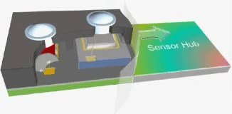
Integrated sensor hub/sensor fusion* has become more and more important in the latest cellphones and wearable devices.
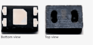
A cavity and functional opening allow environmental sensing.
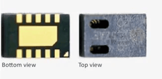
An LGA format supports compact environmental sensor integration.
MEMS and sensor packaging offer modularity, high flexibility and relatively low fabrication complexity, integrating the IC with micro-mechanical components.
Because they are more application-dependent than conventional packaging, they add specific benefits:
Package offerings
ASE offers a variety of sensor packaging solutions that leverage upon an established database of material properties and assembly experience to address dedicated sensor requirements of different microelectronic, optoelectronic, RF, biomedical device, sensor, actuator and microsystem applications.
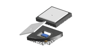
Pressure Sensor
OCQFN (Open Cavity Quad Flat No-lead)
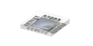
Ambient Light Sensor
OQFN (Optical Quad Flat No-lead)
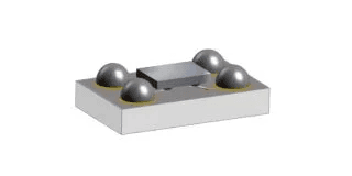
Timing
CoW (Chip on Wafer)
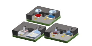
Proximity Sensor
OLGA (Optical Land Grid Array)
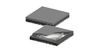
RFIC
PMQFN (Pre-mold Quad Flat No-lead)
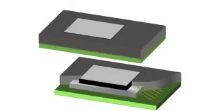
Fingerprint Sensor
iLGA (image Land Grid Array)
LiDAR
ASE offers advanced sensor solutions for the automotive industry, especially LiDAR (light detection and ranging) for autonomous vehicles. LiDAR measures distance and scans the environment accurately: conventional LiDAR sends out infrared light and times how long it takes to bounce off an object and back, building a 3D map; advanced Frequency Modulated Continuous Wave (FMCW) LiDAR can also determine an object's reflectivity and speed (5D). These 3D or 5D maps let autonomous vehicles react promptly and take preventive action.
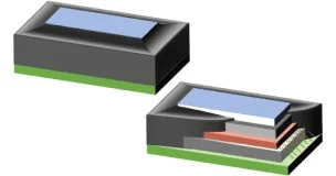
CoW for compound semiconductor & CMOS ROIC integration, spacer for interference immune, glass sealing process, bandpass filter on glass, wire coating
Pre-mold flat lead-frame, plastic lid with glass cover, semi-hermetic sealing
CoW for compound semiconductor & CMOS ROIC integration, double plastic lid for particle resistance, bandpass filter on glass