Overall molding (FCCSP)
Protects the chip, replaces underfill for lower cost, and improves thermal performance and 2nd-level reliability.
Solutions
Flip chip flips the die to connect via solder or gold bumps, spreading I/O pads across the whole chip surface.
That shrinks die size, optimizes the circuit path and cuts signal inductance. An essential step is wafer bumping; ASE can bump 6-, 8- and 12-inch wafers.
One-pass bonding, denser I/O and shorter paths, with direct heat removal and a lower profile.
 Shorter assembly cycle time (all bonding in one process)Higher signal density and smaller die (area-array pad layout)Good electrical performance from the short die-to-substrate pathDirect thermal path for an external heat sinkLower profile (no wire or molding)
ASE offers several BGA packages using flip chip technology.
| Package | I/O | Package size (mm) | Substrate | Ball pitch (mm) |
|---|---|---|---|---|
| CCSP | 16–200 | 4×4 – 14.0×22.0 | 2/4-layer laminate | 0.5–1.00 |
| Ceramic FCBGA / PGA | <1556 | 27×27 – 49.5×49.5 | Ceramic | 0.8–1.27 |
| FCBGA | 100–1521 | 27×27 – 40.0×40.0 | 2/4 laminate, 4–8-layer build-up | 1.0 / 1.27 |
| HFCBGA | 256–2401 | 12×12 – 52.5×52.5 | 4–8-layer build-up | 1.0 / 1.27 |
Protects the chip, replaces underfill for lower cost, and improves thermal performance and 2nd-level reliability.
Adheres to the rear of the die for direct heat conduction; 6–8 W dissipation under natural convection.
Packaging offerings

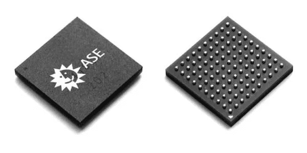
A chip-scale package for around 200 I/O or fewer. FCCSP gives better chip protection and solder-joint reliability than direct chip attach (DCA) or chip on board (COB), and beats known-good die (KGD) for low-cost test and burn-in while performing comparably — in a thin, small, lightweight package.
Laminate and build-up organic substrates provide strong electrical performance for high-frequency computing, network and communications products.
A heat spreader lowers junction-to-case resistance and improves external cooling for high-power devices.