
Solutions
System in Package (SiP)
Overview
A package or module that holds a whole electronic system or subsystem, miniaturized through IC-assembly technologies. ASE leads SiP from design to high-volume manufacturing.
The drive to miniaturize
Semiconductor miniaturization and integration are unleashing the potential of System-in-Package: a package or module that contains a functional electronic system or subsystem, integrated and miniaturized through IC-assembly technologies. It delivers higher performance, cost-effectiveness and shorter time to market across a huge range of electronics.
Where ASE stands
ASE is the leader in SiP, from design and assembly to high-volume manufacturing, serving a broad spectrum of applications and markets.
What is It
What is System-in-Package (SiP)? FOCoS-Bridge?
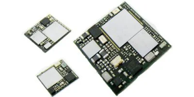
ASE defines SiP as a package or module that contains a functional electronic system or subsystem, integrated and miniaturized through IC-assembly technologies. Unlike generic IC packaging, SiP relies on heterogeneous integration of single or multiple chips (such as a specialized processor, DRAM or flash memory), SMD resistors/capacitors/inductors, filters, connectors, MEMS devices, sensors, other active and passive components, and pre-assembled packages or subsystems.

Enabling Technologies
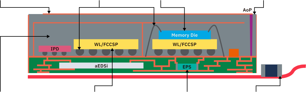
ASE's SiP draws on established IC-assembly capabilities: Copper wiring, flip-chip, wafer-level packaging, fan-out WLP, 2.5D/3D IC and embedded-chip packaging, serving mobile, IoT, HPC, automotive and AI.
Shielding
Conformal Shielding

Compartment Shielding
Selective Shielding
Magnetic shielding
Interconnection
Cap Wire Bond
Wire Bond
Flip Chip
Die / Package Stacking
2.5D
Die Thinning / Stacking
Package on Package
Antenna
Antenna on Package
Antenna in Package
Double Side Molding
Double Side Molding
Selective Molding
Flexible Encapsulation
Molded Underfill
Irregular Packaging
Wafer Level Package
Wafer Bumping
Cu Pillar
Fan-out WLP
Wafer Level IPD
Wafer Level MEMS
Embedded Substrate
SESUB
a-EASI
Board Assembly
High Density SMT
ACF Bonding
Wire Bond on Flex
Laser Welding
Flex Bending
Turnkey Solution
Complete SiP manufacturing capability
ASE offers complete SiP manufacturing capability, including system design, software development, module testing and electrical heat-transfer simulation, to enable smaller, higher-performance, lower-power and more cost-effective products.
System Co-Design
- SiP Electronic Design Automation (EDA) solution
- RF Circuit design
- Antenna Design
- Shielding Solution
- Substrate Layout design
Packaging Consultancy
- Package selection & configuration
- Design rule guideline
- Process capability
- Reliability verification
System Test Consultancy
- RF Wafer probing
- RF ATE Platform
- EVB design & fabrication
- Testing tooling design
- Final test solution development
SiP-id
System-in-Package Intelligent Design (SiP-id)
What SiP-id is
SiP-id is an enhanced reference flow that includes IC-packaging and verification tools from Cadence, plus a methodology that aggregates wafer-, package- and system-level design requirements into one unified, automated flow. It lets chip designers reduce design iterations and greatly improve throughput versus existing advanced-packaging EDA tools, sharply cutting the time to design and verify ultra-complex SiP packages.
Availability
The design tools are available to eligible customers immediately, though some proprietary libraries and design rules are subject to an agreement with ASE. It is an ongoing effort covering fan-out (such as FOCoS), panel fan-out, embedded substrates and 2.5D, as well as making the tools more user-friendly and efficient.
Getting started
A DRC deck is required for fan-out design, and a 3D DRC deck for SiP design. Customers can engage ASE's in-house engineering to begin.


Customer

ASE Team

1
Initiate a package (FOCoS, 2.5D, SiP, etc)
Sales / tech-support teams → ASE site, design / engineering teams

2
Chip package information
Interactive confirmation with customers:
- Chip text in & import netlist
- Package design
- DRC (Design Rule Check)

3
Review drawing
Revising interacitons

4
Confirm drawing
Engineering sample & production
Applications
SiP is widely adopted for wireless communication, computer storage, power and sensor applications.
SiP is widely adopted for wireless communication, computer storage, power and sensor applications, and it enables smart living, smart bike, smart city, smart automotive and smart hearables. ASE develops advanced SMT, encapsulation, shielding and interconnection technologies for 5G communication, AR/VR sensing and healthcare.
Wireless SiP Module
Computing Storage SiP Module
Sensor & Optical SiP Module
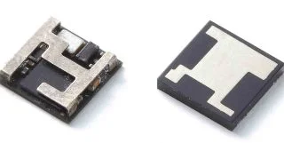
BT/BLE+MCU SiP Module
Applications
- Remote Control
- Health, Fitness and Medical Devices
- Home Automation, Energy
Features
- 2.4 GHz BLE transceiver
- ARM®sup> Cortex – M0 32 bit processor
- 256 kb embedded flash program memory
- 16 kb RAM
- Dimension: 6.5x6.5x1.2mm
- Package: AoP, LGA
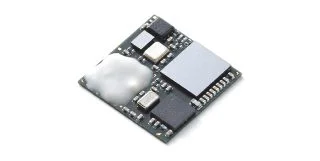
WLAN+MCU SiP Module
Applications
- IoT
- Smart Home
- Security
- Energy Harvesting
Features
- Dimension: LGA 11x11mm²
- Structure: FC+W/B
- WiFi 11b/g + 32bit MCU (50MHz)
- 128kb flash + 512kb EEPROM
- Dimension: 6.5x6.5x1.2mm
- Protection: molding, conformal shielding
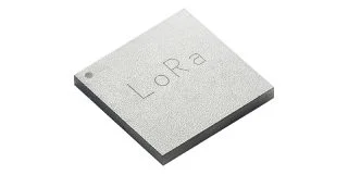
LoRa/SigFox/NB-IoT SiP Module
Applications
- Wireless Alarm and Security Systems
- Internet of Things (IoT)
- Smart City
Features
- SX1276 transceiver
- Intel 32MHz Quark MCU
- DSP for sensor subsystem
- Worldwide LoRa ISM band embedded
- 384 kb of on-die NVM+8 kb OTP on-die NVM
- 80kb of on-die SRAM
- Dimension: 12x12x1.3mm
- Package: Conformal shielding, WLCSP