Solutions
Fan-Out SiP
Overview
Using fan-out RDL as an advanced substrate to push SiP to finer lines, higher performance and lower cost.
System-in-Package has furnished each new mobile generation with higher performance in a smaller form factor for a decade. Multi-functional active chips and passive components are pre-assembled into a system or subsystem through heterogeneous-integration design on a laminated substrate. As SiP moved into mobile devices, cost-effective integrated substrate and small form factor became essential. With existing substrate technology near its limits, fan-out redistribution layers (RDL) become the advanced substrate that breaks through, evolving SiP into Fan-Out SiP.
Features
Several core building blocks enable Fan-Out SiP:
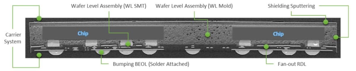
- Fan-out RDL — fine-line design capability better than mainstream substrates, to improve function matching in SiP
- Carrier system — makes thin-wafer handling possible
- Wafer-level assembly — high-speed SMT (>60k units/hour) plus Molded Underfill (MUF) for advanced encapsulation
- Shielding sputtering — an option for specific RF applications
In brief, ASE offers a complete toolbox for Fan-Out SiP packaging.
Benefits
Key Benefits
- Flexible RDL design to tune system performance (versus wire bonding)
- Finer RDL line width and space for higher performance control (about 5x enhancement)
- Substrate-layer reduction (about 3 layers cut)
- Cost-effective wafer-level platform with high-speed SMT (bumping-process compatible)
- Wider RF application via optional five-side sputtering shielding
Applications
The addressable markets:
- Smartphones
- Tablets
- RF infrastructure
- Edge computing
- Internet of Things
Higher-frequency use, better performance and cost-effectiveness are driving package innovation, and Fan-Out SiP provides a platform to meet that demand.