Applications
Silicon Photonics
No longer an emerging technology, but the essential infrastructure of the AI era — the transition from copper to light.

Overview
Data is outgrowing what copper can carry.
In an era where data is generated at an unprecedented rate, the demand for efficient and high-speed data transmission has never been more critical. This demand is driven by advancements in artificial intelligence (AI), the Internet of Things (IoT), and cloud computing, all of which require a robust infrastructure capable of handling massive volumes of data. However, traditional copper wiring, which has long served as the backbone of data transmission, is reaching its physical limits, resulting in what is known as the 'interconnect bottleneck.' This bottleneck occurs when the raw computing power of modern processors exceeds the available bandwidth for data transfer, leaving high-performance chips idle and underutilized.
Advancements in Silicon Photonics (SiPh) mark a significant leap forward in the quest for high-bandwidth, low-power optical transceivers, which are crucial for addressing the 'interconnect bottleneck.' As the industry transitions from traditional pluggable modules to more integrated solutions like Linear Drive Pluggable Optics (LPO), Near-Package Optics (NPO), and Co-Packaged Optics (CPO), we are witnessing a remarkable evolution in optical interconnect technology.
However, this journey is not without its challenges. The complexities of CPO assembly, the precision required for optical coupling, and the need for robust testing methodologies highlight the importance of ongoing research and development in this field. Solutions like 3D integration and wafer-level optical testing offer promising pathways to overcome these obstacles, paving the way for scalable and reliable SiPh systems. ASE's advanced networking and co-packaged optics integration solutions are well-positioned to tackle these challenges and support the evolving needs of the semiconductor industry.

trends & innovations
Optics is moving from the panel into the package.
The development of Silicon Photonics (SiPh) aims to leverage the economies of scale of CMOS (Complementary Metal-Oxide-Semiconductor) technology to create high-bandwidth, low-power optical transceivers. This technology enables the creation of light-guiding structures on a silicon-on-insulator (SOI) substrate, facilitating the guiding, splitting, modulation, and detection of light within a silicon photonics integrated circuit (IC). While silicon photonics cannot generate light, it can perform all other necessary functions for a transceiver that transmits and receives digital signals to and from a single-mode fiber optic cable.
Since 2018, silicon photonics-based pluggable optical transceivers have been available to address the needs of next-generation optical interconnection applications. As the industry progresses toward higher data rates, such as 400G and 800G per port, there is a noticeable "contraction" of the data path, which brings light closer to the silicon to mitigate the resistive and capacitive losses associated with copper.
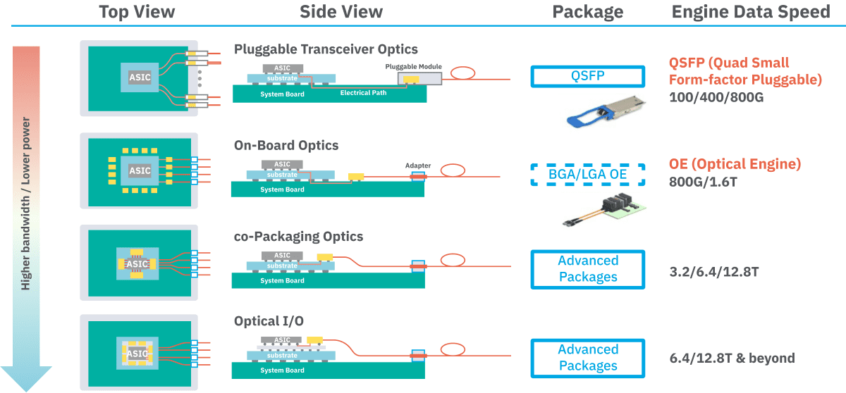
Front panel
Linear Drive Pluggable Optics (LPO)
In a conventional pluggable module, a Digital Signal Processor (DSP) functions as the brain and corrective engine, effectively reducing electrical noise before it reaches the laser. However, the DSP is the largest power consumer within the module, often accounting for up to 50% of the total power usage. LPO eliminates the need for a DSP entirely, leveraging the high-performance SerDes (Serializer/Deserializer) integrated into the host ASIC (such as Broadcom's Tomahawk 5 or NVIDIA's Spectrum-4) to transmit the signal across the PCB.
On-board
Near-Package Optics (NPO)
NPO serves as a transitional solution between traditional pluggable modules and full co-packaging. Instead of placing optics at the front panel, the optical engines (OEs) are relocated to the system board, positioned within 5 cm of an XPU or switch ASIC. This proximity significantly reduces the "trace length" on the PCB, enabling the use of simpler, lower-power drivers and Transimpedance Amplifiers (TIAs).
On-substrate
Co-Packaged Optics (CPO)
CPO represents the final evolution in this integration process. In a CPO architecture, the "Optical Engine" is no longer a standalone component; it is integrated alongside high-performance ASICs (such as switch ASICs or GPUs) within the same package. This integration minimizes electrical paths, resulting in higher bandwidth, reduced power consumption, and enhanced scalability.
On-interposer
Optical I/O — "On Interposer" solutions
The industry is progressing towards more power-efficient and tightly integrated CPO solutions by transitioning from "On Substrate" to "On Interposer" Solutions. In the "OE on Substrate" approach, the optical engine is positioned on the organic package substrate in close proximity to the ASIC, typically within a distance of 10 millimeters. In contrast, the "OE on Interposer" solution utilizes 2.5D packaging technology to directly integrate the optical engines onto the silicon interposer alongside the main ASICs. This drastically shortens electrical trace lengths to just a few millimeters, further enhancing critical metrics such as bandwidth density, power consumption, and latency.
| Technology | Location of optics | Signal conditioning | Typical reach | Power efficiency |
|---|---|---|---|---|
| Pluggable | Front Panel | Full DSP in Module | Up to 10km+ | 20-30 pJ/bit |
| LPO | Front Panel | Host-side SerDes only | < 2km | ~8-10 pJ/bit |
| NPO | On-Board | Host-side / Linear | < 500m | ~20 pJ/bit |
| CPO | On-Substrate | Direct-Drive | < 100m | ~5 pJ/bit |
| Optical I/O | On-Interposer | Direct-Drive | < 100m | ~2 pJ/bit |
Key issues
Three hurdles OSATs must clear.
While Silicon Photonics presents numerous opportunities for the semiconductor industry, it also poses significant challenges, particularly for the outsourced semiconductor assembly and testing (OSAT) sector. These challenges must be addressed to fully realize the potential of Silicon Photonics technology.
Complexity in CPO assembly
In a typical CPO configuration, XPUs or a switch ASIC is centrally located, surrounded by multiple optical engines (OEs). The assembly includes various components such as lasers, optics, fiber array units (FAUs), and silicon integrated circuits (ICs) across different wafer nodes. The OE itself comprises both optical components, like photodetectors and modulators within the Photonic Integrated Circuit (PIC), and electrical components, such as the Driver and Transimpedance Amplifier in the Electronic Integrated Circuit (EIC).
A key challenge in EIC/PIC integration is the presence of parasitics, which can degrade performance. While various packaging solutions exist, 3D integration is particularly effective for reducing trace lengths, thereby minimizing parasitics and enhancing coupling efficiency. As a result, 3D integration is essential for meeting the performance objectives of Co-Packaged Optics (CPO) in terms of bandwidth and power consumption.
Optical alignment and coupling issues
Fiber coupling is a critical and challenging step in CPO, requiring precise alignment with sub-micron accuracy to effectively couple light into the small waveguides on PICs for smooth and efficient light transmission. In traditional pluggable optics, FAUs are connected using butt or grating coupling (GC) through Active Alignment (AA), a time-consuming process that employs real-time feedback to optimize optical coupling before being permanently bonded with epoxy. This method makes repairs impossible if a single fiber fails. While edge coupling (EC) with a V-groove design enables passive alignment (PA), such designs can only be assembled and tested one unit at a time due to structural limitations.
To enhance reparability and upgradability, the industry is moving toward detachable FAU solutions. However, these solutions encounter challenges in achieving sub-micron alignment accuracy and maintaining repeatability across multiple mating cycles while also meeting high-volume manufacturing (HVM) requirements. One promising approach involves using wafer-level optical couplers to enlarge the laser beam size, significantly increasing coupling tolerance and facilitating more scalable assembly.
Optical testing challenges
In a CPO (Co-Packaged Optics) system, the failure of a single optical engine can result in the loss of the entire switch ASIC module or xPU module. This underscores the critical need for reliable and scalable testing processes. Ensuring the quality and performance of optical components is vital for their widespread adoption in the industry. The absence of cost-effective testing methodologies can lead to inconsistencies in product quality and reliability.
A preferred approach is double-sided electro-optical wafer-level testing, which allows simultaneous interfacing with one side of the wafer through Automatic Test Equipment (ATE) while connecting the other side via detachable optical sockets. This method is essential for validating 3D optical engines prior to final assembly. However, the lack of industry standards for FAU (Fiber Array Unit) connectors and testing methodologies complicates the development of universal automated test systems.
ASE technology platform
VIPack™ brings the EIC and PIC together in 3D.
VIPack™ — Photonic 3D
VIPack™ supports advanced networking and co-packaged optics integration, enabling higher I/O bandwidth density and lower energy per bit. We have successfully demonstrated a CPO device that overcomes the integration challenge of assembling multiple optical engines with an ASIC in a large-format package. For networking, our CPO solution presents a viable alternative to current faceplate-pluggable (FPP) solutions. For compute applications, it enables the integration of CPUs, GPUs, and XPUs with optics into a single, high-speed co-packaged solution.
The 3D integration of EIC/PIC typically follows a 3D Heterogeneous Integration flow, leveraging Through-Silicon Vias (TSVs), Middle-End-Of-Line (MEOL) processing, Chip-on-Wafer (CoW) bonding, and final on-substrate integration.
TSV MEOL of the PIC interposer
The PIC serves as the foundational carrier, providing both optical waveguides for signal routing and electrical TSVs for vertical connectivity between the EIC and the package substrate. The MEOL phase is critical for preparing these vertical interconnects. Typically, "blind" TSVs are formed in the PIC wafer in advance during the front-end foundry process. Then, ASE performs the MEOL process to functionalize these TSVs. This includes: The PIC wafer is ground and etched from the backside until the "blind" TSVs are exposed. Once revealed, a passivation layer is applied, followed by the creation of Backside (BS) Redistribution Layers (RDL) and bumps.
Chip-on-Wafer (CoW) assembly
The Chip-on-Wafer (CoW) stage is where the heterogeneous integration of electronic and photonic components occurs at the wafer level. ASE provides advanced interconnect technologies, such as micro bumps or Cu pillar bumps, to enable the integration of the EIC on top of the PIC. After bonding, underfill is applied to enhance thermal and mechanical reliability. In some architectures, a molding compound may be formed to protect the delicate chiplet interfaces. The resulting Photonic 3D architecture provides ultra-short electrical paths which offer superior thermal management and supports data transmission rates exceeding 200G per lane. This configuration also facilitates testing before the wafer is singulated into individual "Optical Engines."
To enable optimized optical coupling, ASE provides a high-accuracy bonding process to precisely attach optical couplers on the PIC wafer, aligning them perfectly with tapered waveguides or grating couplers. Both PIC local warpage and the beam angle between the PIC & the optical coupler are precisely controlled during attachment. This helps to establish a detachable optical interface between Fiber Array Units (FAUs) and PICs, facilitating wafer-scale testing, supporting detachable FAUs, and reducing sensitivity to wavelength variations. Additionally, the PIC can feature a pre-formed cavity to enable edge coupling, ultimately supporting Dense Wavelength Division Multiplexing (DWDM) systems.
On-substrate integration
The final stage of CPO assembly involves mounting the singulated Optical Engines onto a package substrate, typically larger than 120x120mm. The optical engines are integrated alongside the main ASIC/Switch die on the substrate. In the "on-interposer" architecture, the ASIC and optical engines share a single silicon interposer, which is then placed onto the main package substrate.
A critical final step in the on-substrate process is FAU attachment, where fibers are aligned and connected to the optical couplers and PIC waveguides to form the external optical interface. Because CPO integrates high-power electronics with temperature-sensitive photonics, the final on-substrate design must accommodate high-performance heat sinks or cold plates to ensure operational reliability.
Conclusion
The essential infrastructure of the AI era.
Silicon Photonics is no longer an "emerging technology"; it is the essential infrastructure of the AI era. The transition from copper to light is a physical necessity dictated by the limits of energy dissipation and signal integrity. As we have explored, the innovations in Co-Packaged Optics and Heterogeneous Integration are reshaping the industry, yet they also introduce significant challenges in 3D packaging, optical coupling, and testing. For OSAT companies, this presents a multi-billion dollar opportunity to ascend the value chain. For the industry as a whole, embracing these advancements is the only viable path to sustaining the AI revolution. As we approach 2030, the leaders will be those who can most effectively harness the speed of light in their packaging solutions.