Solutions

Electrical Lab

Overview

The ASE Electrical Lab (E-Lab) designs, analyzes and characterizes IC-package electrical behavior through simulation and measurement.

E-Lab works with customers on package design optimization, system-level SI/PI analysis, high-speed and high-frequency verification, and turnkey passive-filter solutions. It also offers accurate measurement for package characterization, electrical failure analysis, and chip- and system-level mmWave antenna-in-package (AiP).
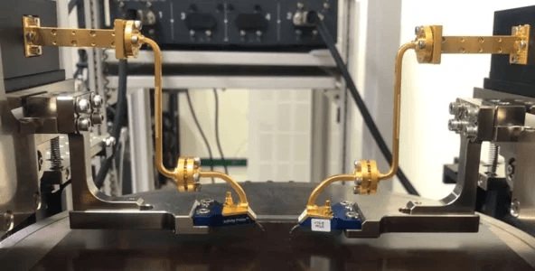
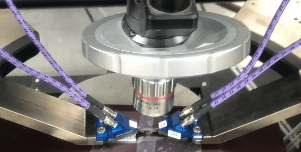
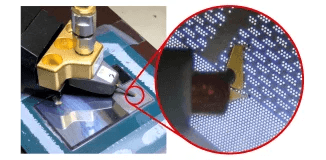
Electrical laboratory probing equipmentElectrical package measurement equipment

services

Design & simulation service

Plastic BGA (PBGA)

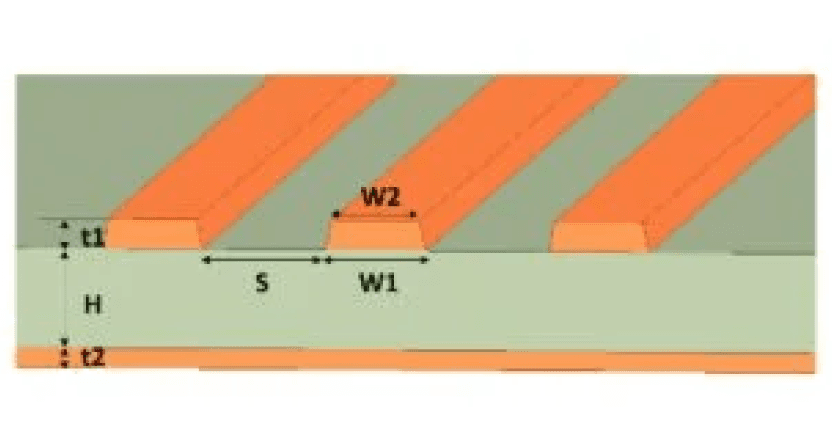
  • Impedance
  • Package design optimization (DDR, SerDes, Power…)
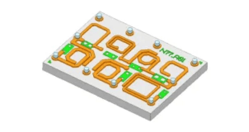
  • RF filter design & characterization
  • Package EMI shielding design (conformal, compartment)

fcCSP Substrate

  • Package R/L/C modeling
  • S-parameter modeling
  • IBIS / SPICE / S-param model export

BOC (DDR substrate)

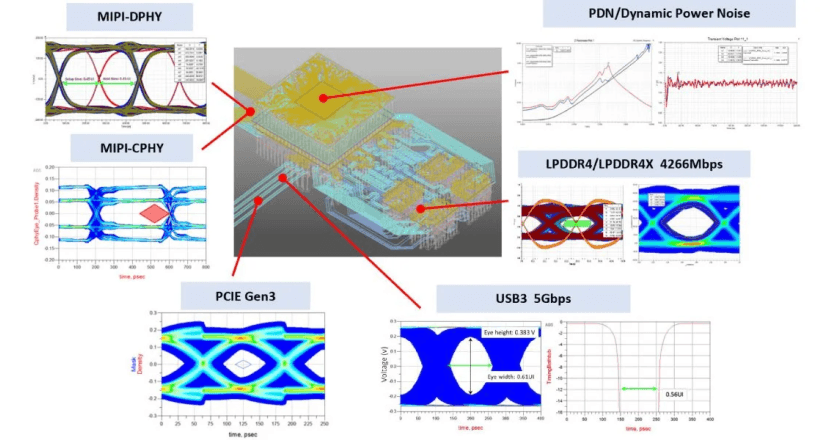
Signal integrity

  • TDR simulation
  • Eye diagram
  • Crosstalk / jitter / timing analysis

Power integrity

  • DCIR drop
  • PDN
  • De-cap optimization
  • Power noise

services

Measurement service

S-parameter

  • Up to 170 GHz double-side probe station
  • Up to 260 GHz single-side probe station
  • 12-inch wafer & panel-level probe station

Electrical FA

  • TDR impedance
  • 4-wire DCR (open / short)

Parasitic

  • Component level
  • On-chip capacitor
  • RF inductor

services

Antenna-in-Package (AiP) service

Spherical chamber

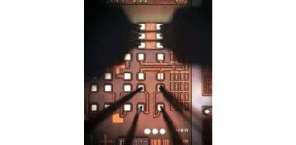
Chip/package-level passive test with a probing feed.
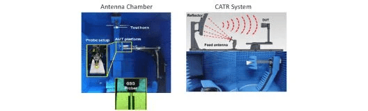
  • Spherical & direct far field
  • Frequency 18–110 GHz
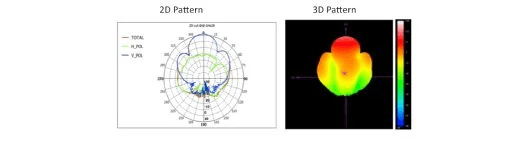
  • Antenna gain, 2D pattern

Compact Antenna Test Range (CATR)

System-level active test with a connector feed.

  • Quiet zone 30×30 cm²
  • Frequency 18–110 GHz
  • Antenna gain, EIRP, 3D pattern
  • Beamforming test

See Other labs

We use cookies to run this site and, with your consent, to measure how it is used. See our Cookie Policy and Privacy Policy.