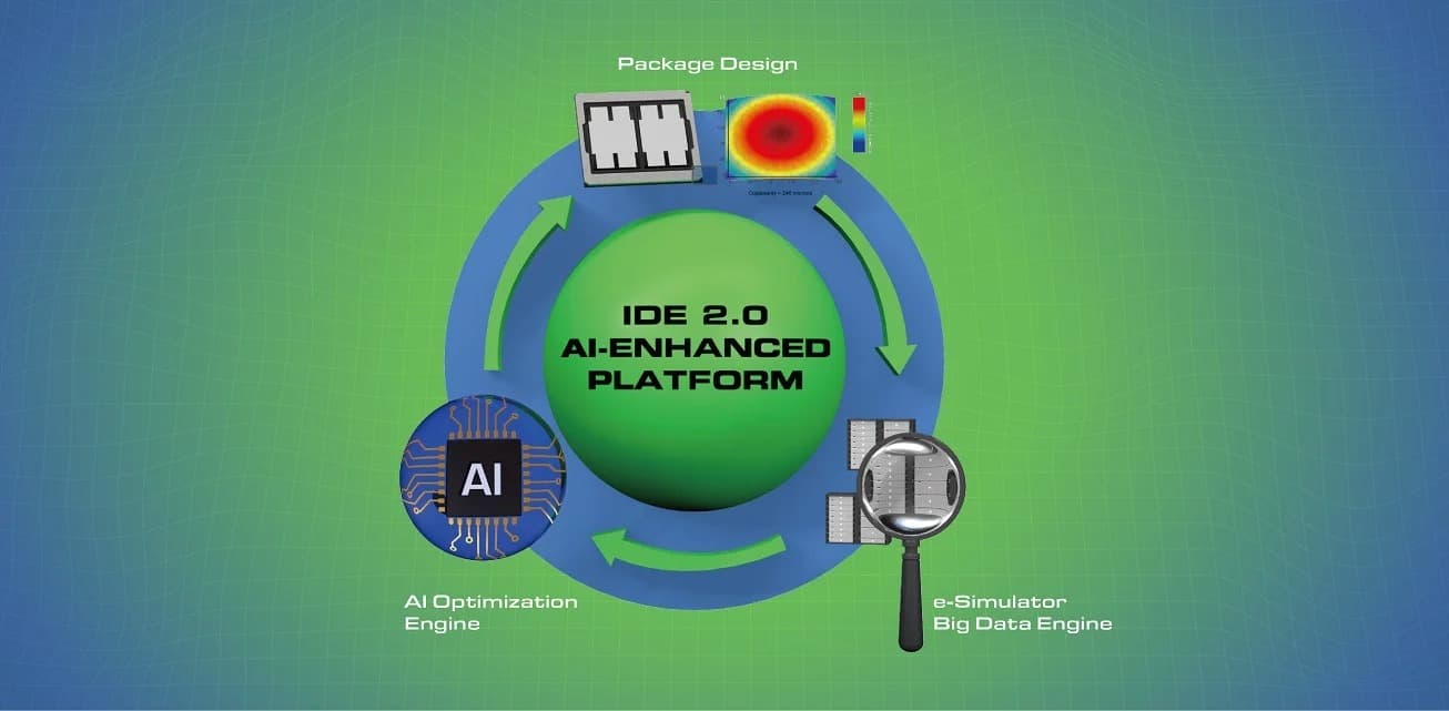
SUNNYVALE, Calif., Nov. 4, 2025 – Advanced Semiconductor Engineering, Inc. (ASE), a member of ASE Technology Holding Co., Ltd. (NYSE: ASX, TAIEX: 3711), today announced the launch of IDE 2.0, a major upgrade to its Integrated Design Ecosystem™ platform. The enhanced platform integrates artificial intelligence to enable faster design iterations, optimize chip-package interaction analysis, and accelerate time to market for complex AI and HPC applications.
Through its new cloud-based e-Simulator, IDE 2.0 uses AI engines to perform predictive risk assessments and optimize design, analysis, and manufacturing data. The platform reduces design cycles while enabling greater precision, performance, and streamlined workflows.
IDE 2.0 introduces an AI-driven feedback framework that continuously connects design and analysis in real time. Combining multiphysics simulation, real-world data, and AI insights improves speed, precision, and reliability across multi-die, chiplet, and heterogeneous-integration technologies.
The workflow enables rapid evaluation of package configurations across mechanical, electrical, and thermal domains, shortening the design-analysis cycle from weeks to hours while protecting customer intellectual property.
Key performance highlights
- Simulation acceleration: Reduces design iteration time by more than 90%, cutting a 14-day process to 30 minutes within defined parameters.
- Integrated multiphysics simulations: Enhances accuracy across electrical, thermal, warpage and stress, and reliability domains.
- AI-based risk prediction: Generates predictive assessments within 60 seconds, enabling real-time design optimization.
“By integrating characterized material and simulation databases with AI-driven capabilities, IDE 2.0 delivers precise insights into chip-package interaction and residual stress,” said Dr. C.P. Hung, Vice President of Corporate Research & Development at ASE.
“The evolution from automated IDE 1.0 to intelligent IDE 2.0 demonstrates the power of AI in advancing ASE’s integrated design ecosystem,” added Yin Chang, Executive Vice President at ASE.
ASE IDE 2.0 is part of VIPack™, ASE’s scalable advanced packaging platform aligned with future technology roadmaps. It is available now as an exclusive collaborative design toolset for ASE customers.
About ASE, Inc.
Advanced Semiconductor Engineering, Inc. (ASE), a member of ASE Technology Holding Co., Ltd. (NYSE: ASX, TAIEX: 3711) is the leading global provider of semiconductor manufacturing services in assembly and test. Alongside a broad portfolio of established assembly and test technologies, ASE is also delivering innovative VIPack™, advanced packaging, and system-in-package solutions to meet growth momentum across a broad range of end markets, including AI, automotive, 5G, high-performance computing, and more.
To learn about our advances in SiP, fanout, MEMS and sensor, flip chip, and 2.5D, 3D and TSV technologies, all ultimately geared towards applications to improve lifestyle and efficiency, please visit the ASE Website, or follow us on LinkedIn and X: @aseglobal.