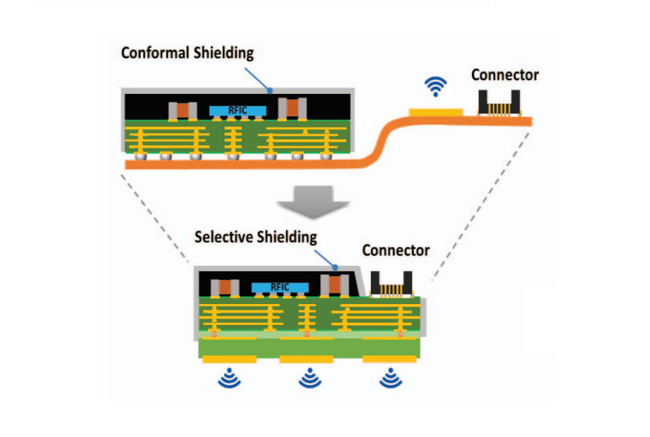
System-in-Package (SiP) module with higher component density and smaller form size was demonstrated through selective structure. The selective EMI shielding at partial molding area for specific substrate circuit exposure through roller-type auto taping / detaping of PI tape was performed. This PI tape was applied on to designed area and form a co-shape masking through package singulation. The sacrification PI tape was successively removed after sputter deposition and no sputter issue such as burnmark, overflow and glue residue was found. Finally, the SMT quality of connector mount was also confirmed and all meet criteria of mass production.
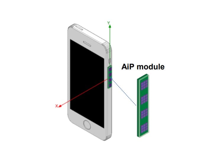
In this study, new selective patterning of EMI shielding was performed through roller-type column taping and detaping. This auto taping and detaping combo system inspired by correction tape provide a excellent taping quality with no bubble trapped and no solder damage. Based on the conformal taping, no further burnmark and overflow was found under even high UPH process and cost benefit than unit taping process with single nozzle. Additionally, zero sputtering shift at 3 sides of package was obtains by co-shape masking defined in singulation process and the high accuracy requirement of pre-formed PI tape was also alleviated by which cost benefit of material was highlighted. In further connector solderability test in SMT, soldering quality with no bridge and no void as well as solder bond strength was meet criteria through shear test. The full process was also passed engineering qualification with extremely low defect rate and show a highly potential to be introduced to the incoming 5G AiP Process.
Published in: 2024 IEEE 74th Electronic Components and Technology Conference (ECTC)